Product added to cart
Lattice MXO2-1200 Small System FPGA Development Board
$0.0000
Out of stock
SKU
MIC-05-011
Shop with confidence Learn More
 Intel Altera Cyclone® IV EP4CE6E22C8N FPGA Development Board Previous
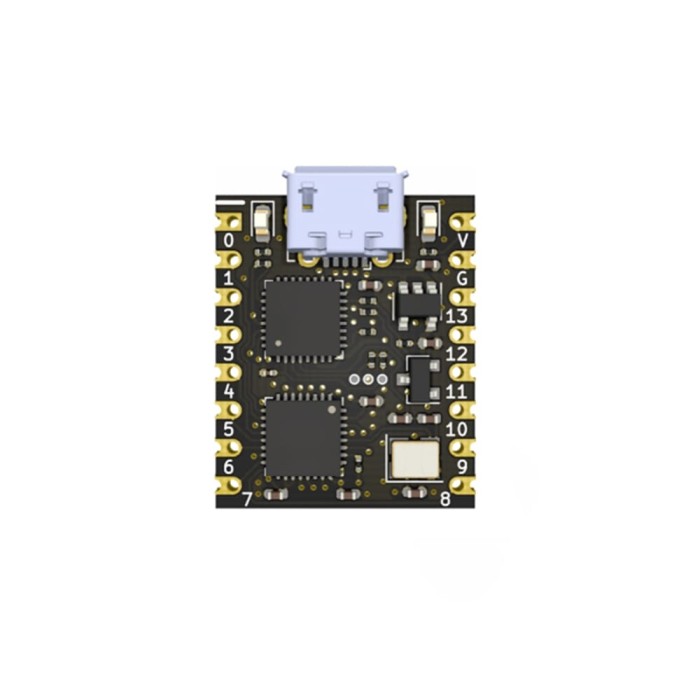
Introducing the Lattice MXO2-1200 Small System FPGA Development Board - a versatile and powerful tool for FPGA development projects. This development board is equipped with the Lattice MXO2-1200 FPGA, providing ample resources for designing and implementing complex digital systems. With its compact size and user-friendly interfaces, it is suitable for both beginners and experienced engineers.
The Lattice MXO2-1200 FPGA offers 1200 Look-Up Tables (LUTs) and 64Kbits of embedded memory, allowing for the creation of sophisticated digital circuits. The development board also features a range of interfaces, including HDMI, USB, and SD card, enabling seamless integration with various peripherals. With its onboard programming capabilities and JTAG support, programming and debugging your FPGA designs is a breeze. Unlock your creativity and unleash the full potential of FPGA technology with the Lattice MXO2-1200 Small System FPGA Development Board.
Experience the power and flexibility of the Lattice MXO2-1200 Small System FPGA Development Board. Whether you're a student, hobbyist, or professional engineer, this board offers the resources and features needed to bring your FPGA projects to life. With its compact design, rich interface options, and powerful FPGA chip, you can prototype, test, and deploy advanced digital systems with ease. Boost your FPGA development capabilities with the Lattice MXO2-1200 Small System FPGA Development Board and embark on your journey of digital innovation.
Specification of Lattice MXO2-1200 Small System FPGA Development Board:
- Lattice-based XO2-1200HC FPGA
1280 LUTs
64Kbits embedded block RAM
a PLL
Support DDR/DDR2/PDDR
Built-in dual-boot Flash is used to configure FPGA
There are 2 I2C, 1 SPI and a timer hard core inside
3.3V power supply
- Powered by MicroUSB, supports DAPLink mode for FPGA configuration and UART communication
- With a 12MHz external clock, the FPGA can operate at high speed through the internal PLL (the test uses a 400MHz clock to generate DDS). The reason for choosing the 12MHz clock is to be able to share it with the LPC11U35 to save costs;
- 14 GPIO pins, the 14th pin is shared with the heartbeat LED on the board;
- 2 LEDs on the board:
A 3.3V power indicator - PWR
One FPGA logic status indicator - HB, used to verify the FPGA logic
- There is a 5V-3.3V LDO on the board , which can be powered externally through PIN 16, with a maximum of 150mA.
Write Your Own Review


Please complete your information below to login.
Sign In
Create New Account