
Product added to cart

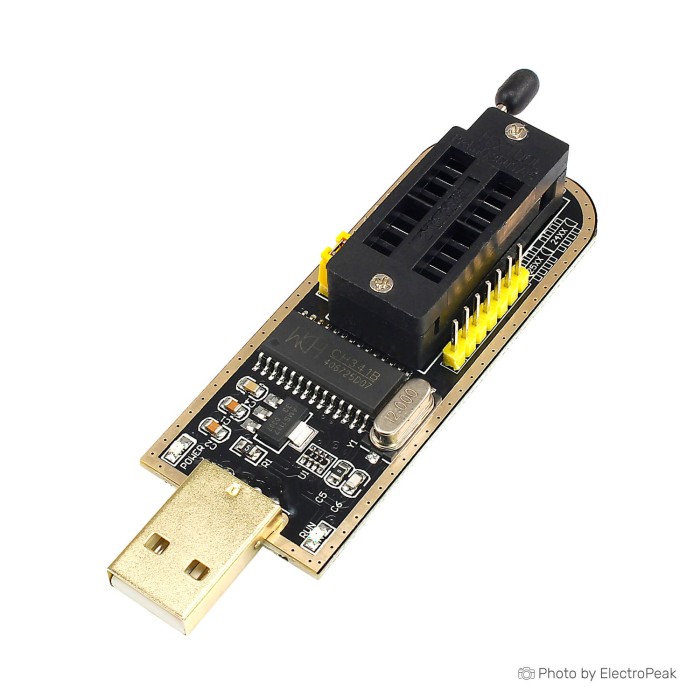
CH341A EEPROM Flash BIOS USB Programmer
$2.0400
In stock
SKU
PRO-01-020
Volume discounts:
- +50 4 % $1.9600
- +100 6 % $1.9200
- +300 8 % $1.8700
- +500 10 % $1.8300
- +1000 12 % $1.7900
Ships in 2-3 business days, then:
Free delivery in 12-15 days by Tracked Economic Shipping on orders over $100.
Free delivery in 7-10 days by Express Shipping on orders over $300.
More shipping info

Shop with confidence Learn More
 USBasp - USB programmer for Atmel AVR controllers Previous
CH341A Programmer Review: BIOS and EEPROM Flashing
The CH341A EEPROM Flash BIOS USB Programmer is a compact USB hardware tool for reading, erasing, and writing 24xx-series I2C EEPROMs and 25xx-series SPI flash memory chips. It suits technicians, hobbyists, and PC repairers recovering corrupted motherboard, video-card, or router firmware when an external memory device must be reprogrammed outside the operating system. Generic boards vary in their power and logic implementations, so this tool is best suited to buyers who can identify their specific memory chip markings and verify voltage requirements before connecting hardware.
This unit is not a universal IC programmer for microcontrollers or complex logic devices. For projects involving non-serial memories, microcontrollers, or devices with proprietary programming protocols, browse our selection of other programming tools to match your target device. For serial memory work, the baseline technical specifications are listed below.
Specifications of CH341A EEPROM Flash BIOS USB Programmer
- Controller chip: CH341A
- Communications: USB 1.1
- Supported memory families: 24xx Series EEPROM and 25xx Series SPI flash chips
- Supported chip configurations: 8-pin or 16-pin configurations
- Operating systems: Win/Linux/MAC
- Power supply: Use USB port power supply
- Power output protection: 500mA fuse ( with fuse version )
- In-circuit programming: Capable of in-circuit programming
- Size: 85mm x 28mm x 12mm
- Intended use: Very suitable for amateur programmer 24 and 25 series FLASH
- Programming-speed claim: Programming is faster than ordinary ATMEGA8
- ATMEL supported storages: AT24C01 AT24C01B AT24C01A AT24C02A AT24C02; AT24C04 AT24C02B AT24C04B AT24C04A AT24C08A; AT24C08B AT24C16A AT24C16B AT24C08 AT24C16; AT24C32 AT24C64 AT24C64A AT24C32B AT24C32A; AT24C128A AT24C128B AT24C256B AT24C64B AT24C128; AT24C256 AT24C512 AT24C256A AT24C512B AT24C512A; AT24C1024 AT24C1024A AT24C1024B
- CATALYST supported storages: CAT24C01 CAT24WC01 CAT24WC02 CAT24C02 CAT24C04; CAT24WC04 CAT24WC08 CAT24C08 CAT24WC16 CAT24C16; CAT24WC32 CAT24C32 CAT24WC64 CAT24C64 CAT24WC128; CAT24C128 CAT24WC256 CAT24C256 CAT24C512 CAT24WC512; CAT24C1024 CAT24WC1024
- COMMON supported storages: 24C01 24C01 3V 5V 5V 24C04 24C02 24C02 3V 5V; 24C04 24C08 3V 3V 5V 24C08 24C16 24C16 3V 5V; 5V 24C32 24C32 24C64 3V 5V 5V 24C64 3V 24C128; 24C256 24C128 3V 5V 5V 24C512 24C512 24C256 3V 3V; 3V 24C1024 24C1024 24C2048 3V 5V 5V 24C2048 24C4096 5V; 24C4096 3V
- FAIRCHILD supported storages: FM24C01L FM24C02L FM24C03L FM24C04L FM24C05L; FM24C08L FM24C09L FM24C17L FM24C16L FM24C32L; FM24C64L FM24C128L FM24C256L FM24C512L FM
- HOLTEK supported storages: HT24C01 HT24LC01 HT24C02 HT24LC02 HT24C04; HT24LC04 HT24C08 HT24LC08 HT24C16 HT24LC16; HT24LC32 HT24C32 HT24LC64 HT24C64 HT24C128; HT24LC128 HT24C256 HT24LC256 HT24LC512 HT24C512; HT24C1024 HT24LC1024
- ISSI supported storages: IS24C01 IS24C02 IS24C04 IS24C08 IS24C16; IS24C32 IS24C64 IS24C128 IS24C256 IS24C512; IS24C1024
- MICROCHIP supported storages: MIC24LC014 MIC24AA01 MIC24AA014 MIC24LC01B MIC24LC02B; MIC24AA02 MIC24C02C MIC24AA025 MIC24AA04 MIC24LC04B; MIC24LC024 MIC24AA024 MIC24LC025 MIC24LC08B MIC24AA08; MIC24LC16B MIC24AA16 MIC24LC32 MIC24AA32 MIC24LC64; MIC24FC64 MIC24AA64 MIC24FC128 MIC24AA128 MIC24LC128; MIC24AA256 MIC24LC256 MIC24FC256 MIC24AA512 MIC24LC512; MIC24FC512 MIC24AA1024
- NSC supported storages: NSC24C02L NSC24C02 NSC24C64
- RAMTRON supported storages: FM24CL04 FM24C04A FM24CL16 FM24C16A FM24CL64; FM24C64 FM24C256 FM24CL256 FM24C512
- ROHM supported storages: BR24L01 BR24C01 BR24L02 BR24C02 BR24L04; BR24C04 BR24L08 BR24C08 BR24L16 BR24C16; BR24L32 BR24C32 BR24C64 BR24L64
- ST supported storages: ST24C01 ST24C02 ST24C04 ST24C08 ST24C16; ST24C32 ST24C64
- XICOR supported storages: X24C01 X24C02 X24C04 X24C08 X24C16
CH341A Programmer Compatibility and Specifications Explained
Often called a "BIOS programmer," the CH341A is intended for a common application rather than a universal hardware standard. BIOS and UEFI firmware chips use serial flash memory, but their electrical interfaces and protocol requirements vary across generations. The CH341A handles two distinct communication families: 24xx-series I2C EEPROMs, such as configuration storage chips, and 25xx-series SPI flash memories, commonly used for system firmware. Attempting to program parallel flash, microcontrollers, or non-serial storage devices directly with this unit will not work.
For Atmel microcontrollers rather than serial flash, use the USBasp AVR ISP Programmer, which is designed for AVR and ATtiny ISP programming through direct SPI in-system headers. The CH341A is for external memory chips, not MCU execution flash.
Support for 8-pin and 16-pin devices means the pin routing accommodates standard dual-in-line layouts. Most modern computer motherboards and graphics cards, however, use surface-mount SOP8 or SOIC8 BIOS chips. Programming these without desoldering requires an external test clip, such as a SOP8 to DIP8 clip, to bridge the surface-mount contacts to the programmer's connection headers.
| Specification | Listed Value | Why It Matters |
|---|---|---|
| Target Protocols | 24xx I2C / 25xx SPI | Restricts compatibility to serial EEPROM and SPI flash. Does not program microcontrollers or parallel NOR/NAND flash chips. |
| Bus Interface | USB 1.1 | Provides broad host compatibility across older and modern USB ports. Transfer throughput is limited by USB 1.1 speeds, making larger flash chips (16MB+) take several minutes to read or write. |
| Form Factor | 85mm x 28mm x 12mm | Compact physical footprint suitable for bench use, though physical clearance around onboard headers depends on your wiring setup. |
| Device Packages | 8-pin or 16-pin configurations | Accommodates standard DIP layouts directly; surface-mount chips (SOP8, SOP16, WSON8) require corresponding adapters or clip assemblies. |
| Host Platforms | Win / Linux / MAC | Communicates across platforms, but actual operation depends on selecting host software (e.g., AsProgrammer, NeoProgrammer, or flashrom) compatible with your OS environment. |
Before ordering, read the complete part number etched on your physical chip. The extensive compatibility list covers standard I2C EEPROMs from manufacturers such as Atmel, Microchip, and ST, but SPI flash chips must be verified individually against your target flashing software database to confirm that erase and write algorithm parameters match.
CH341A Voltage Safety and Known Limitations
Voltage matching is critical when working with serial flash memory. Many contemporary SPI flash chips on motherboards, laptops, and networking gear are rated for 3.3 V or 1.8 V operation. Early hardware revisions of black CH341A boards were documented in the hardware community as supplying 3.3 V to the target power pin (VCC) while leaving the SPI and I2C signal lines tied to the 5 V USB rail. Subjecting 3.3 V memory chips to 5 V logic signals can cause thermal stress or permanent silicon damage.
Generic boards come from varied production runs, so the precise board revision, trace layout, and onboard voltage circuitry are not uniform across the market. Review these operational limitations before applying power:
- Signal Voltage Verification: Use a digital multimeter to measure both the supply pin (VCC) and the communication lines (CS, CLK, MOSI, MISO) relative to ground before clipping onto a sensitive 3.3 V memory chip.
- 1.8 V Flash Devices: The base programmer does not provide 1.8 V supply or signal levels out of the box. Flashing 1.8 V serial flash requires a dedicated level-shifting adapter that actively translates both the power rail and all logic signals down to 1.8 V.
- Power Protection Variance: The specification notes a 500mA fuse on "fuse version" revisions. Because board builds differ, do not rely on onboard fusing to protect against misaligned wiring or target-board shorts.
- Automatic Detection Limitations: Software auto-detection works by querying the chip's JEDEC ID. High-resistance wiring or target-board components that clamp the lines will cause detection to fail or return erroneous 0x00 or 0xFF readings.
CH341A BIOS Flashing and First Read Verification
Flashing a corrupted BIOS chip demands a strictly verified workflow. Writing to a memory chip is destructive; if you erase the flash before obtaining a verified backup of the original image, device recovery becomes significantly more difficult. Follow this baseline sequence when setting up a read or write operation:
- Identify the Chip: Clean the package surface and read the complete part marking under direct light. Identify whether it operates at 3.3 V or 1.8 V.
- Confirm Signal Voltages: Plug the programmer into your computer without the target chip attached, then measure the socket pins with a multimeter to confirm signal voltage levels.
- Isolate Target Power: If you are programming in-circuit on a motherboard or device, disconnect all power sources, remove the main battery, and disconnect the CMOS coin cell. Never apply external power to a board while attaching the programmer.
- Align Pin 1: Locate pin 1 on the chip, indicated by an indented dot or beveled edge, and align it with pin 1 on the socket or test clip. Misaligned connections prevent detection and risk overheating the chip.
- Extract Two Backups: Use your chosen utility, such as AsProgrammer, NeoProgrammer, or flashrom, to read the chip. Save the file, perform a second independent read, and compare the SHA-256 or MD5 checksums of both files. They must match bit-for-bit.
- Write and Verify: Once matching backups are secured, load the clean firmware binary, execute the erase/write routine, and run the software verify pass to confirm the written flash matches the source file.
For detailed step-by-step instructions on driver configuration and utility setup, refer to our BIOS flashing guide.
When in-circuit programming fails, indicated by verify errors or chips reading entirely as 0x00 or 0xFF, surrounding motherboard circuitry is sinking current from the programmer's data lines. In these circumstances, the only reliable fallback is to desolder the chip and place it directly into a socket or breakout adapter.
CH341A Programmer Accessories and Package Requirements
The programmer unit provides the core USB interface and socket headers, but recovery and repair jobs require auxiliary hardware based on how the target chip is mounted. Review your setup requirements before starting work:
- Required — Host Machine and Software: A computer with an available USB port running Windows, Linux, or macOS. You need programming software capable of driving the CH341 hardware backend, such as AsProgrammer, NeoProgrammer, or flashrom.
- Required — Connection Interface: Standard DIP-package chips fit directly into the onboard socket. Surface-mount devices require an adapter board or external test clip matched to the chip's physical footprint.
- Required — Verified Binary and Backup Storage: A reliable local drive to store dual binary backups before executing any write operations, alongside the target firmware image.
- Recommended — In-Circuit Clip: For surface-mount memory soldered directly to a PCB, a dedicated SOP8 to DIP8 clip lets you contact the pins directly on the board without immediate desoldering.
- Recommended — Measurement Tools: A digital multimeter to check supply and logic-level voltages on the programmer headers before connecting sensitive components.
- Optional — 1.8 V Active Level Shifter: Mandatory if your target chip is a 1.8 V SPI flash, common in low-power laptops and newer PC platforms. This adapter must actively shift both supply voltage and data lines.
- Optional — SMD Rework Station: A soldering iron or hot-air rework station with flux and wick, necessary when in-circuit parasitic loads prevent reliable reading and the chip must be removed from the host board.
CH341A Programmer FAQ: BIOS Chip, Driver, and 1.8V Questions
Will this CH341A programmer work with my motherboard or laptop BIOS chip?
It works only when the BIOS chip uses a supported serial protocol, such as 25xx SPI flash, matches the programmer's operating voltage, and is recognized by your programming software. Check the physical part number on the chip against your utility's device list before connecting.
Is the CH341A safe for 3.3 V BIOS chips?
Electrical safety depends on the specific PCB revision. Early generic black boards supplied 3.3 V on the power pin while driving the data lines at 5 V, which can stress 3.3 V flash devices. Measure the socket's data and power pins with a multimeter before connecting your target chip.
Can this CH341A programmer flash a 1.8 V BIOS chip?
Not without a separate 1.8 V level-shifting adapter. Connecting a 1.8 V flash device directly to the programmer's native headers risks burning out the chip due to overvoltage on both the VCC rail and data lines.
Do I need to remove the BIOS chip from the board?
In-circuit programming is supported, but success depends on the surrounding motherboard circuit. If capacitors, pull-up resistors, or the host chipset interfere with the SPI bus, reads return unstable data or verify errors, requiring you to desolder the chip for off-board flashing.
Does this programmer include a SOP8/SOIC8 clip or 1.8 V adapter?
Package contents vary across production runs, and supplementary adapters or test clips are not guaranteed unless explicitly bundled. If you are flashing surface-mount chips in place, add a dedicated SOP8 to DIP8 clip to your order.
Why does a CH341A show no chip or read FF/00?
Reading all 0x00 or 0xFF indicates an open or short circuit on the data lines. Common causes include poor clip contact on oxidized chip legs, reversed pin-1 orientation, insufficient target power, driver-mode conflicts, or target-board components loading down the clock and data signals.
Which software works with the CH341A programmer?
On Windows, community utilities such as AsProgrammer and NeoProgrammer are standard choices for serial flash. Linux and macOS environments frequently use flashrom or IMSProg. Ensure your operating system has the correct USB driver backend assigned to interface with the CH341 chip.
For bare PIC microcontroller development rather than serial memory, a multi-socket board such as the PICKIT Programming Socket Board provides DIP footprint routing for PIC microcontroller programming with dedicated PIC hardware tools.
Why should I make two backups before writing BIOS firmware?
A single read can appear structurally complete even when poor pin contact has corrupted occasional bytes. Comparing two independent reads using cryptographic checksums confirms that bus communication was stable and guarantees a faithful recovery image before you erase the chip. Review our BIOS flashing guide for backup verification practices.
CH341A Programmer Buying Checklist and Decision Summary
The CH341A programmer is an accessible, effective tool when used within its operational boundaries. Review the criteria below to confirm whether this device fits your technical requirements:
- Ideal for: Technicians and hobbyists working with clearly identified 24xx I2C EEPROMs or 25xx 3.3 V SPI flash chips who can verify socket voltages and operate utilities such as AsProgrammer or flashrom.
- Maybe for: Users flashing soldered 8-pin BIOS chips with a test clip, provided they understand that circuit interference may require desoldering if read verification fails.
- Avoid if: You need plug-and-play programming for 1.8 V chips without auxiliary adapters, require guaranteed logic-level protection out of the box, or need to flash microcontrollers rather than external serial memories.
For firmware flashing and debugging on ARM Cortex-M or 8-bit STM devices, use dedicated hardware debugger such as the Waveshare ST-LINK V2 Mini, which provides SWIM and SWD interfaces designed for STM8 and STM32 programming.
Before purchasing, confirm each item on this verification checklist:
- I have read the physical part number from the target memory chip.
- The chip is confirmed as a 24xx-series EEPROM or 25xx-series SPI flash memory.
- I have checked whether the chip requires 3.3 V or 1.8 V operating levels.
- If the chip is 1.8 V, I have sourced an active bidirectional level-shifting adapter.
- I have a multimeter available to verify the programmer's pin voltages prior to connection.
- I have the necessary SOP8 clip or socket adapter for my chip's physical package.
- My target operating system supports utilities capable of driving the CH341A backend.
- I have established a workflow to capture and verify two matching read backups before attempting an erase or write cycle.
For tools covering different architectures, memory types, or hardware debug interfaces, browse our catalog of other programming tools to select the correct hardware for your bench.
| Interface Type | USB, UART, I2C, SPI |
|---|---|
| Operating Voltage (V) | 5V |
| Operating Current (mA) | 500 |
| Operating Temp (°C) | -40 to 85 |
| Dimensions (mm) | 85 x 28 x 12mm |
| Mounting Type | Direct connection to chips |
| Interface Category | USB to TTL Converter |
| Output Type | USB |
| Chipset | CH341 |
| Voltage Range | 3.3V - 5V |
| Protocols | I2C, SPI, UART, USB |
| Conversion Type | USB to TTL |
Write Your Own Review

Please complete your information below to login.
Sign In
Create New Account