Product added to cart
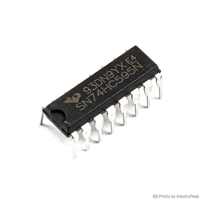
74HC595 Shift Register
$0.0458
In stock
SKU
ELC-01-013
74HC595 Shift Register is available to buy in increments of 10
Ships in 2-3 business days, then:
Free delivery in10-15 days by YunExpress on orders over $35.
Free delivery in5-7 days by DHL on orders over $200.
More shipping info
Shop with confidence Learn More
 Atmega168-PU 8-bit IC Microcontroller Previous
Description
The 74HC595; 74HCT595 is an 8-bit serial-in/serial or parallel-out shift register with a storage register and 3-state outputs. Both the shift and storage register have separate clocks. The device features a serial input (DS) and a serial output (Q7S) to enable cascading and an asynchronous reset MR input. A LOW on MR will reset the shift register. Data is shifted on the LOW-to-HIGH transitions of the SHCP input. The data in the shift register is transferred to the storage register on a LOW-to-HIGH transition of the STCP input. If both clocks are connected together, the shift register will always be one clock pulse ahead of the storage register. Data in the storage register appears at the output whenever the output enable input (OE) is LOW. A HIGH on OE causes the outputs to assume a high-impedance OFF-state. Operation of the OE input does not affect the state of the registers. Inputs include clamp diodes. This enables the use of current limiting resistors to interface inputs to voltages in excess of VCC.
Features
8-bit serial input
8-bit serial or parallel output
Storage register with 3-state outputs
Shift register with direct clear
100 MHz (typical) shift out frequency
Complies with JEDEC standard no. 7A
Input levels:
For 74HC595: CMOS level
For 74HCT595: TTL level
ESD protection:
HBM JESD22-A114F exceeds 2000 V
MM JESD22-A115-A exceeds 200 V
Multiple package options
Specified from 40C to +85C and from 40C to +125C
Write Your Own Review


Please complete your information below to login.
Sign In
Create New Account