
Product added to cart

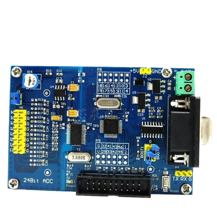
ADS1256 24-bit ADC Module with Serial Output
$18.9500
In stock
SKU
MOD-10-011
Volume discounts:
- +25 4 % $18.2100
- +50 6 % $17.8400
- +100 8 % $17.4700
- +300 10 % $17.1100
- +500 12 % $16.7400
Ships in 2-3 business days, then:
Free delivery in 12-15 days by Tracked Economic Shipping on orders over $100.
Free delivery in 7-10 days by Express Shipping on orders over $300.
More shipping info

Shop with confidence Learn More
 CH343P High Speed USB to TTL (Serial) Module With Type-C Connector Previous
ADS1256 24-bit ADC Module review: who it is for
Priced at $18.95, this development board combines an ADS1256 24-bit, 8-channel analog-to-digital converter with an onboard STM32F103C8T6 microcontroller that streams conversion data through a serial UART connection. Integrated voltage regulators, anti-reverse power protection, and an onboard test potentiometer make it a practical platform for intermediate embedded developers building precision data-acquisition setups. It is not intended for plug-and-play eight-channel data logging, direct USB-based flashing, or measuring negative single-ended voltages without external signal conditioning.
The converter connects directly to the onboard microcontroller rather than being exposed as an external SPI peripheral, so integration centers on serial communication or flashing custom STM32 firmware. Among our ADC and converter modules, this board suits systems where an intermediate microcontroller offloads the conversion workload. For the same hardware configuration under a secondary catalog entry, see the identical ADS1256 24-bit ADC Module.
Specifications of ADS1256 24-bit ADC Module with Serial Output
- Dimensions: 82.8 x 53.4 x 1.6mm
- Chip Model: STM32F103C8T6 (MCU), ADS1256 (24-bit ADC)
- Power Supply Voltage: 5V and 3.3V on-board regulators; 9V external DC power supply
- Crystal Frequency: 8MHz (internal frequency 72MHz)
- Channels: 8 (24-bit)
- Reference Voltage: 2.5V (generated by precision voltage regulator)
- Programming Interface: Serial port (no JLINK interface)
- Test Function: Potentiometer for AD input testing (AN0-AN7)
- Power input terminal input voltage range: 5.5V - 12V
- USB to TTL connection: MCU TX, RX, GND
- Imported 3232 serial port communication chip
- JTAG interface
- STM32F103C8T6 reset button
- STM32 BOOT0 and BOOT1 select control jump cap
ADS1256 24-bit ADC Module specifications explained
The onboard hardware determines whether this board fits your system architecture or adds unexpected firmware overhead.
| Specification | Hardware Implementation | Why It Matters in Practice |
|---|---|---|
| Microcontroller Architecture | STM32F103C8T6 (ARM Cortex-M3, 72MHz core) | The microcontroller manages ADS1256 configuration, sample timing, and data output internally. You do not talk directly to the ADC over SPI from a Raspberry Pi or external board; you communicate with the STM32 over serial. |
| Serial Interface | UART via TX, RX, and GND; onboard 3232 transceiver chip | Allows direct streaming to a PC or secondary host using an external 3.3V USB-to-TTL adapter or through RS-232 serial circuitry. No native USB controller is present on the board. |
| Power Supply Input | 5.5V to 12V terminal, 5V direct input terminal, onboard 5V & 3.3V regulation | Offers flexibility when powering from a bench supply, 9V battery, or industrial DC bus. Anti-reverse diode protection prevents damage from reversed polarity, but only one supply path should be connected at a time. |
| Voltage Reference | 2.5V generated by onboard precision regulator | Establishes the analog measurement baseline. The 2.5V nominal voltage is fixed on the board, but specific temperature drift, component tolerance, and long-term stability ratings are unlisted, so metrology work requires external calibration. |
| Test Potentiometer | Onboard adjustable trimmer tied to analog channel AN0 (AIN0 / I0) | Enables immediate analog input testing right out of the box without connecting external sensors or signal sources. This speeds up serial communication checks. |
| GPIO & Boot Controls | Accessible STM32 GPIO pin headers, BOOT0/BOOT1 jumper caps, hardware reset button | Provides full access to unused microcontroller peripherals for custom embedded firmware development, sensor triggering, or status LEDs using standard STM32 serial bootloader workflows. |
During breadboard bring-up of the serial output and analog inputs, a reliable Breadboard Jumper Wire Kit helps prevent intermittent connection faults on the 2.54mm header pins.
ADS1256 ADC board limits: inputs, channels, and noise
High-resolution converters demand careful analog frontend design. The ADS1256 silicon provides 24-bit raw conversions across up to eight single-ended channels, but physical circuit constraints and firmware behavior determine real-world performance.
Input Voltage Range and Buffer Behavior
The board does not support direct negative voltages on any analog terminal. Single-ended input voltages must remain strictly between AGND (0V) and 5V. Enabling the internal ADS1256 analog input buffer in firmware increases input impedance, but narrows the allowable single-ended input range to approximately 0V through 3V (specifically, AVDD minus 2.0V). An analog input above 3V with the buffer enabled causes signal clipping. With differential signals, the difference between positive and negative inputs can be calculated algebraically, but neither individual input pin may drop below ground.
Out-of-the-Box Channel Streaming vs. Custom Firmware
The board contains eight physical 24-bit conversion channels, but the factory-installed demo firmware continuously reads only AN0 and transmits that single channel's data over serial. Monitoring channels AN1 through AN7, reading differential pairs, or modifying the sampling rate requires writing and flashing custom firmware onto the STM32F103C8T6. Multiple-channel multiplexing must respect ADC settling times and digital filter synchronization; switching channels on a sigma-delta converter reduces effective throughput compared with continuous single-channel sampling.
24-Bit Resolution vs. Usable Precision
A 24-bit resolution mathematically divides the reference span into 16,777,216 discrete steps, but that does not equal 24 bits of noise-free accuracy. Under optimal conditions at low sample rates, such as 2.5 to 30 SPS, real-world usable resolution on the ADS1256 typically reaches between 21 and 23 noise-free bits. At the chip's maximum 30 kSPS sampling rate, thermal and digital noise increase significantly. Unshielded wiring, power-supply ripple, and uncharacterized reference drift on generic boards further restrict effective precision unless proper shielding, external filtering, and calibration are applied.
For projects focused entirely on weight scales or static strain gauges rather than multi-channel data acquisition, the specialized HX711 Load Cell Amplifier Module provides a dedicated differential front end with lower system complexity.
ADS1256 STM32 serial setup and first test
This board has no native USB port or integrated USB-to-serial bridge, so connecting it to a computer requires an external 3.3V USB-to-TTL serial adapter. A 5V adapter can overstress the STM32 logic pins.
Initial Wiring and First-Power Bring-Up
- Provide power using either a regulated 5V DC supply on the 5V terminal or a 5.5V to 12V DC supply on the main power terminal block. Do not connect power to both inputs simultaneously.
- Connect your 3.3V USB-to-TTL adapter to the board: adapter TX connects to board MCU RX, adapter RX connects to board MCU TX, and adapter GND connects to board GND. Ensure common ground is established.
- Verify that the BOOT0 and BOOT1 jumper caps are set to their default operating positions (BOOT0 set to 0) for executing factory firmware.
- Open a serial terminal program on your computer. With the factory demo firmware running, the board transmits ASCII voltage readings corresponding to channel AN0.
- Rotate the onboard test potentiometer with a small screwdriver and confirm that the reported voltage in the serial assistant rises and falls across the adjustment range.
Flashing Custom Firmware via Serial Bootloader
Acquiring multiple channels or adjusting conversion parameters requires custom code compiled for the STM32F103C8T6. Move the BOOT0 jumper cap to 1, press the onboard reset button to enter the STM32 system memory bootloader, and upload your compiled binary over the serial UART pins using standard STM32 flashing utilities. After the upload finishes, move the BOOT0 jumper back to 0 and press the reset button to run the new firmware. Custom SPI routines must properly manage the ADS1256 DRDY signal line and include the required setup delays after channel multiplexing commands.
ADS1256 ADC board vs ADS1115 and ADS1232
The right analog conversion module depends on host interface requirements, resolution needs, and whether you want an integrated MCU or a direct bus breakout.
| Feature | ADS1256 STM32 Module | ADS1115 4-Channel ADC | ADS1115 with Ferrites | ADS1232 Differential ADC | AD7705 SPI ADC |
|---|---|---|---|---|---|
| Resolution | 24-bit | 16-bit | 16-bit | 24-bit (up to 23.5 effective bits) | 16-bit |
| Analog Inputs | 8 single-ended / 4 differential | 4 single-ended / 2 differential | 4 single-ended / 2 differential | 2 differential channels | 2 differential channels |
| Host Interface | UART Serial (via onboard STM32) | I2C | I2C (4 selectable addresses) | 2-wire serial interface | SPI |
| Maximum Sample Rate | Up to 30 kSPS (ADS1256 single-channel) | 8 SPS to 860 SPS | 8 SPS to 860 SPS | 10 SPS or 80 SPS | Low-frequency configurable |
| Onboard Controller | STM32F103C8T6 MCU onboard | None (Bare breakout) | None (Bare breakout with ferrites) | None (Bare breakout) | None (Bare breakout) |
| Internal Gain / PGA | PGA up to 64 | PGA up to 16 | PGA up to 16 | PGA up to 128 | PGA up to 128 |
Consider how your host controller will collect data before choosing between these architectures:
- For simple Arduino-based monitoring of thermistors or battery levels at moderate speeds, the ADS1115 16-Bit 4-Channel ADC connects directly through I2C and has broad library support. Our guide on interfacing the ADS1115 with Arduino lets you evaluate that workflow.
- Multiple I2C converters on one bus with improved power rail filtering call for the ADS1115 Breakout with Ferrites, which provides address configuration pins and onboard inductive filtering.
- Dedicated weigh scales, load cells, or bridge sensors that require low-noise differential sampling and gains up to 128 suit the ADS1232 24-Bit Differential ADC, which offers an optimized signal path. See our tutorial on interfacing the ADS1232 with Arduino for hardware connection details.
- For compact industrial control circuits that favor direct microcontroller SPI communication without intermediary firmware, the AD7705 16-Bit SPI ADC is a 16-bit dual-channel alternative.
- Choosing one of the separate breakout converters above instead of this integrated STM32 board? Pairing it with an Arduino Uno R3 (Clone) provides a reliable prototyping platform for testing SPI or I2C sensor communications.
ADS1256 24-bit ADC Module accessories and wiring
The module does not include connection cables or an external host bridge, so completing a data-acquisition setup requires several supporting components.
Required Accessories
- 3.3V USB-to-TTL Serial Adapter: Required to bridge the board's MCU TX, RX, and GND pins to a computer USB port for serial monitoring and firmware flashing.
- DC Power Supply: A clean DC power source delivering 5.5V to 12V to the main power terminal, or a regulated 5V source connected to the 5V terminal.
- Analog Input Wiring: Solid copper leads or sensor wiring with a clean common ground reference to AGND.
Recommended Accessories
- Prototyping Wires: The Breadboard Jumper Wire Kit - 140 Pieces provides pre-stripped, color-coded jumpers for serial adapters, analog test voltages, and supply lines.
- Solderless Breadboard: An 830 points Breadboard provides a stable base for assembling voltage dividers, low-pass RC filters, or sensor conditioning networks before routing signals to the screw terminals.
- Shielded Twisted-Pair Cable: Essential on long analog runs to prevent ambient electromagnetic noise from corrupting high-resolution measurements.
- Signal Conditioning Components: Precision resistor dividers or op-amp buffers for measuring voltages exceeding 5V or high-impedance signal sources.
Optional Accessories
- Precision Voltage Calibrator: A stable external voltage source for verifying and calibrating ADC readings against board reference drift.
- External STM32 Debugger: An SWD/JTAG hardware programmer when in-circuit breakpoint debugging is required instead of serial bootloader flashing.
ADS1256 ADC board FAQ
Can I read all 8 channels out of the box?
No. The board has eight 24-bit physical input channels, but the factory-installed firmware continuously reads only channel AN0 and transmits that single stream over serial. Reading channels AN1 through AN7 requires developing and uploading custom firmware to the onboard STM32 microcontroller.
What voltage can the ADS1256 ADC board measure?
Single-ended analog input voltages must remain between 0V and 5V relative to ground. With the ADS1256 internal input buffer active, the single-ended measurement span narrows to roughly 0V through 3V. Input pins must never be exposed to negative voltages below AGND.
Is this really accurate to 24 bits?
The converter outputs 24-bit integer values, but usable, noise-free resolution is lower in practical systems. Effective resolution depends heavily on sample rate, power supply filtering, input signal impedance, board layout, and temperature stability, typically reaching 21 to 23 noise-free bits at low sampling speeds.
Does this board connect directly to Arduino or Raspberry Pi over SPI or I2C?
No. The ADS1256 SPI lines route directly to the onboard STM32F103C8T6 microcontroller. External host devices communicate with the board through the UART serial pins (TX, RX, and GND) rather than accessing the ADC chip directly over an SPI bus.
Does the ADS1256 ADC Module have USB programming?
No. The board has no USB connector or built-in USB-to-UART converter. Programming the STM32 microcontroller requires an external 3.3V USB-to-TTL serial adapter connected to the MCU serial pins while managing the BOOT0 jumper and reset button.
Why do readings stop near 3V or 3.3V?
This happens when the internal ADS1256 analog input buffer remains enabled. Buffer-on operation restricts the common-mode input range to AVDD minus 2V, approximately 3V when powered from a 5V analog rail. Disabling the buffer in firmware restores the full 0V to 5V input range, though input impedance will be lower.
Can I use this board for a load cell?
Yes, but it requires external effort. The ADS1256 provides differential inputs and programmable gain up to 64, but this module lacks a built-in bridge excitation circuit or pre-configured scale firmware. For dedicated weigh scale development, consider the purpose-built HX711 Load Cell Amplifier Module or the ADS1232 24-Bit Differential ADC. For an equivalent secondary listing of this exact module, refer to the ADS1256 24-bit ADC Module.
What is the onboard potentiometer for?
The trimmer potentiometer is hardwired to analog input channel AN0 (AIN0 / I0). It serves as an adjustable reference voltage divider, allowing you to verify that the ADC, microcontroller, and serial output stream operate correctly before wiring external sensors.
Is a J-Link debugger included?
No. The board does not include a J-Link debugger. JTAG pads or header markings may exist on the PCB, but primary code deployment is designed around the STM32 serial UART bootloader using standard BOOT0 jumper selection.
Purchase Decision Summary
| Ideal For | Maybe For | Consider Another Option If |
|---|---|---|
|
|
|
Buying Checklist
- I have confirmed that system communication relies on UART serial output rather than direct host SPI or I2C buses.
- I have a 3.3V USB-to-TTL serial adapter available for computer connection and firmware programming.
- I understand that the stock firmware reads channel AN0 only, and multi-channel acquisition requires custom STM32 code.
- My input signals stay within 0V to 5V (or 0V to 3V with the analog buffer enabled) and never drop below ground.
- I have factored in that multi-channel multiplexing and serial ASCII formatting reduce real-world throughput below the 30 kSPS chip maximum.
- I have an appropriate DC power source (5.5V to 12V on the main terminal or regulated 5V) and know not to connect both simultaneously.
- I have verified that the physical PCB dimensions of 82.8 x 53.4 x 1.6mm fit my enclosure or mounting plate.
| Interface Type | UART |
|---|---|
| Dimensions (mm) | 82.8 x 53.4 x 1.6mm |
| Interface Category | Converter |
| Output Type | UART |
| Channels | 8-channel |
| Chipset | STM32F103C8T6, ADS1256 |
| Voltage Range | 5.5V - 12V |
| Protocols | UART |
| Conversion Type | Analog to Digital |
Write Your Own Review

Please complete your information below to login.
Sign In
Create New Account