

Introduction
If you’re working with the ESP8266 pinout, first determine whether you mean the bare ESP8266 chip/module or a NodeMCU development board. That distinction affects GPIO availability, ADC range, boot behavior, and even which pins are broken out to headers.
This guide focuses on the NodeMCU ESP8266 board pinout, while also showing where the bare ESP8266 IC and ESP-12F module differ. The goal is simple: help you choose the right pins the first time, avoid boot issues, and get the board running in Arduino IDE without guesswork. If you want a board-first setup walkthrough, see this guide on getting started with NodeMCU ESP8266 in Arduino IDE.

Key Takeaways
- ESP8266 vs NodeMCU board scope and version differences
- Safe GPIO selection and boot-sensitive pins
- NodeMCU ESP8266 pinout and peripheral capabilities
- ADC, SPI, I2C, UART, PWM, and interrupt pin usage
- Arduino IDE setup for programming NodeMCU ESP8266
Is ESP8266 the same as NodeMCU? Different Versions of NodeMCU ESP8266
ESP8266 is a WiFi microcontroller from the ESP family that requires external flash memory and an antenna. Different modules and development boards were built around this microcontroller.
What is a Development Board?
A development board wraps the main IC with the support hardware you need for easier use: power regulation, USB-to-serial, headers, buttons, and usually better labeling.
NodeMCU is actually an IoT platform and firmware that runs on the ESP8266. In practice, though, ESP8266 development boards that use this ecosystem are commonly called NodeMCU boards.

So ESP8266 and NodeMCU are not the same thing. ESP8266 is the chip or module family. NodeMCU usually refers to the development board built around it.
If you need the module by itself rather than a full dev board, the ESP-12F ESP8266 Wi-Fi module exposes the same core ESP8266 family behavior, but not the same header layout as NodeMCU.
Board Scope: Which Pinout This Article Covers
The main pinout in this article applies to the popular 30-pin NodeMCU ESP8266 development board. Bare ESP8266 ICs and modules do not expose the same pins in the same way, even though the underlying chip behavior is similar.
That matters most in three areas:
- which GPIOs you can physically access
- which pins are tied to onboard flash
- whether the ADC input is the raw chip input or the NodeMCU board-level A0 input
ESP8266 Pinout
Before wiring a sensor, relay, display, or serial device, check whether the pin is safe at boot and whether the board already uses it for flash, SPI, or USB serial.
Warning
Check the safe GPIO summary before wiring peripherals. A poor pin choice can block boot or conflict with flash-connected and serial pins.
Safe-to-Use GPIOs vs Caution/Avoid Pins
This is the quick decision table most projects need.
| Board Pin | GPIO | Best Use | Boot Behavior / Restriction | Recommendation |
|---|---|---|---|---|
| D0 | GPIO16 | Simple digital I/O, wake from deep sleep | HIGH at boot; no interrupt as routine input; no I2C support; PWM not recommended (RTC domain; can cause resets) | Use with caution |
| D1 | GPIO5 | General digital I/O, default I2C | No boot restrictions | Best choice |
| D2 | GPIO4 | General digital I/O, default I2C | No boot restrictions | Best choice |
| D3 | GPIO0 | Digital I/O only if boot state is controlled | Connected to FLASH button; boot fails if pulled LOW | Use with caution |
| D4 | GPIO2 | Digital I/O, UART1 TX | HIGH at boot; boot fails if pulled LOW | Use with caution |
| D5 | GPIO14 | Digital I/O, HSPI clock | Shared with SPI use case | Good if SPI not needed |
| D6 | GPIO12 | Digital I/O, HSPI MISO | Shared with SPI use case | Good if SPI not needed |
| D7 | GPIO13 | Digital I/O, HSPI MOSI | Shared with SPI use case | Good if SPI not needed |
| D8 | GPIO15 | SPI chip select, output with care | Must be LOW at boot; boot fails if pulled HIGH | Use with caution |
| RX | GPIO3 | UART0 RX, input if necessary | HIGH at boot; used for flashing and debugging | Use with caution |
| TX | GPIO1 | UART0 TX, output if necessary | HIGH at boot; boot fails if pulled LOW; used for flashing and debugging | Use with caution |
| GPIO6–GPIO11 labels vary | GPIO6–GPIO11 | Flash interface | Connected to flash memory / internal SPI flash bus | Avoid |
| A0 | ADC0 | Analog input only | Analog input only, not a digital output | Special-purpose only |
ESP8266 Peripherals and I/O Overview
The ESP8266 supports several functions on a small set of pins, so the same GPIO can appear in more than one section. That is normal. The chip uses pin multiplexing, and software can assign or remap some functions depending on the library and interface.
| Function | Available On NodeMCU ESP8266 | Default Pins / Notes |
|---|---|---|
| GPIO | Yes | Multiple GPIOs exposed on the 30-pin board |
| ADC | 1 channel, 10-bit | A0 on NodeMCU board |
| UART | 2 ports exposed in part | UART0 on RX/TX; UART1 transmit only on GPIO2/D4 |
| SPI | Yes | User-facing HSPI on D5, D6, D7, D8 |
| I2C | Yes, by software convention | Commonly D2 as SDA and D1 as SCL; can be remapped with
Wire.begin(SDA, SCL) |
| PWM | Yes | PWM available on most GPIO0 through GPIO15 pins; GPIO16 not recommended for PWM |
| Interrupts | Yes, except GPIO16 | GPIO16 does not support external interrupts |
| I2S | Yes | Supported by ESP8266 |
Datasheet and Pinout For ESP8266 IC


For the manufacturer reference, competitor material also cites the official ESP8266 datasheet.
ESP8266 Pinout And Datasheet (ESP8266-12F Module)

NodeMCU ESP8266 Pinout (Amica/DoIT, LoLin Brands)
This guide describes the pins of the NodeMCU ESP8266 development board, which follows the same core behavior as the ESP8266 module.
Amica/DoIT models are the second generation of NodeMCU development boards, while the LoLin model is the third generation.

Today, the most common versions are LoLin and Amica. They differ slightly in board dimensions and in the function of two header pins: on LoLin V3, pin 3 is a 5 V output, while on Amica V2 the same physical position is labeled RSV (reserved, not connected). All other GPIO and peripheral behavior is the same.

If you are choosing between board variants, the NodeMCU ESP8266 CP2102 Wi-Fi development board and the NodeMCU ESP8266 V3 Lua CH340G Wi-Fi development board are the same board family for most pinout decisions, but they use different USB-to-serial chips.
NodeMCU Specifications

Main Components on NodeMCU ESP8266 Board

NodeMCU ESP8266 Pinout And Specifications; All in One Look
This image makes a good desk reference if you use the board often.

ESP8266 Pinout: Suitable Pins for Digital I/O
For general digital I/O, start with the least risky pins. That keeps boot behavior predictable and leaves shared interface pins available if you need them later.
First Priority
The best pins for general digital I/O are:
- D1 (GPIO5)
- D2 (GPIO4)
These are the safest defaults for switches, LEDs, simple sensors, and control signals.
Second Priority
These pins can also work well as digital I/O if you do not need SPI for the project:
- D5 (GPIO14)
- D6 (GPIO12)
- D7 (GPIO13)
Third Priority
These pins can be used, but only if you control their boot state carefully:
- D3 (GPIO0)
- D4 (GPIO2)
The boot process uses both pins. If external hardware pulls them to the wrong level during boot, the board may not start.
D3 and D4 are especially risky with relays, transistors, optocouplers, and driver circuits because those parts can force the line HIGH or LOW before firmware takes control.
Other Pins Which Are Not Recommended to Use
- TX / GPIO1 can work as an output, but it is also the UART transmit line to the computer. It is HIGH during boot, and pulling it LOW can stop boot.
- RX / GPIO3 can work as an input, but it is also the UART receive line used for programming and serial communication. It is HIGH at boot.
- D0 / GPIO16 is limited. It has no interrupt as a routine input and does not support I2C. PWM on this pin is not recommended due to RTC domain limitations. It is also HIGH at boot.
- D8 / GPIO15 can work as an output, but the board will not boot if it goes HIGH during boot.
ESP8266 Pinout: ADC Pins with Arduino IDE
The NodeMCU board gives you one analog input: A0. That is enough for reading a potentiometer, an analog sensor output, or any other single voltage signal that fits the input range.
Warning
Do not assume every ESP8266 analog input accepts 0–3.3V. The bare ESP8266 chip/module ADC limit is lower than the NodeMCU board-level A0 input, so applying NodeMCU assumptions to a bare module can damage hardware.
ADC Range: Bare ESP8266 vs NodeMCU A0
- The ESP8266 chip or module ADC is 0–1V
- The NodeMCU board A0 pin is commonly 0–3.3V
- The NodeMCU board reaches that wider A0 range by using resistive division on the board
| Context | Input Label | Expected Range | Important Limitation |
|---|---|---|---|
| Bare ESP8266 chip/module | ADC | 0–1V | Do not apply NodeMCU A0 0–3.3V assumptions here |
| NodeMCU ESP8266 development board | A0 / ADC0 | 0–3.3V | Board-level scaling is on the development board, not the bare chip |

ADC Supply-Voltage Measurement Limitation
According to the ESP8266 datasheet, the ADC can be configured to measure either:
- the external analog input, or
- the supply voltage of VDD3P3
but not both at the same time.
That matters if you plan to reuse the ADC for battery or rail monitoring. Treat A0 as a single shared ADC resource.
The only analog input on the NodeMCU ESP8266 board is A0 (ADC0). In the example below, the board reads the potentiometer wiper voltage and prints the value to the serial monitor.
Schematic and Code

					#include <Arduino.h>
void setup()
{
    Serial.begin(9600);
}

void loop()
{
    Serial.print("ADC Value: ");
    Serial.println(analogRead(A0));
    delay(300);
}
ESP8266 Pinout: SPI Pins
The ESP8266 exposes both flash-related SPI signals and user-facing SPI pins. Do not treat them as the same thing.
Reserved Flash/SDIO Pins (GPIO6–GPIO11)
These pins are tied to the onboard flash interface and should be avoided for external wiring on NodeMCU boards.
| GPIO | Common Label | Connected To | External Use Recommendation |
|---|---|---|---|
| GPIO6 | CLK | Flash memory | Avoid |
| GPIO7 | SD0 / MISO | Flash memory | Avoid |
| GPIO8 | SD1 / MOSI | Flash memory | Avoid |
| GPIO9 | SD2 | Flash memory | Avoid |
| GPIO10 | SD3 | Flash memory | Avoid |
| GPIO11 | CMD / CS | Flash memory | Avoid |
On the left side of the pinout image, these pins are used for internal SPI communication with flash memory and have practically no external use.

User-Facing HSPI Pins
The NodeMCU board provides four practical SPI pins for external devices:- D5 (GPIO14) — HSCLK, SPI clock
- D6 (GPIO12) — HMISO, MISO
- D7 (GPIO13) — HMOSI, MOSI
- D8 (GPIO15) — HCS, chip select

Example: SPI Communication between NodeMCU Board and Arduino UNO
In this example, the Arduino UNO is the SPI slave and the NodeMCU board is the master. The slave receives the string"Hello UNO" and prints it to the serial port.
Schematic

Code for NodeMCU as a Master
					#include <Arduino.h>
#include <SPI.h>

char buff[] = "Hello UNO\n";
void setup()
{
    SPI.begin(); /* begin SPI */
}

void loop()
{
    for (int i = 0; i < sizeof(buff) - 1; i++) // transfer one byte per second
    {
        SPI.transfer(buff[i]); // transfer byte i from buffer buff on SPI line
        delay(1000);
    }
}
Code for Arduino UNO as a Slave
ESP8266 Pinout: I2C Pins
For most NodeMCU projects, start with D1 and D2 for I2C. They are the common default pairing and the least confusing option when you are using existing Arduino examples.
					#include <Arduino.h>
#include <SPI.h>

char buff[100];
volatile byte index;
volatile bool receivedone; /* use reception complete flag */

// SPI interrupt routine
ISR(SPI_STC_vect)
{
    uint8_t oldsrg = SREG;
    cli();
    char c = SPDR;
    if (index < (sizeof buff - 1))
    {
        buff[index++] = c;
        if (c == '\n')
        { /* Check for newline character as end of msg */
            receivedone = true;
        }
    }
    SREG = oldsrg;
}

void setup(void)
{
    Serial.begin(9600);
    SPCR |= bit(SPE);                                    /* Enable SPI */
    pinMode(MISO, OUTPUT); /* Make MISO pin as OUTPUT */ // <<---*** in slave device MISO must to define OUTPUT
    index = 0;
    receivedone = false;
    SPI.attachInterrupt(); /* Attach SPI interrupt */ // activate spi interrupt
}

void loop(void)
{
    if (receivedone) /* Check and print received buffer if any */
    {
        if (index >= sizeof buff)
            index = sizeof buff - 1;
        buff[index] = 0;
        Serial.println(buff);
        index = 0;
        receivedone = false;
    }
}
Info
Default I2C Pins and Remapping
The common default I2C mapping on NodeMCU is:
- D2 (GPIO4) — SDA
- D1 (GPIO5) — SCL
ESP8266 does not have fixed hardware I2C pins in the same sense many MCUs do. Instead, I2C can be handled in software, and you can move it to other GPIO pairs when needed.

I2C Communications between NodeMCU and Arduino UNO using Arduino IDE Software
In this example, the NodeMCU board acts as the I2C master and the Arduino UNO acts as the slave. Each side sends a short string and prints the received data to the serial monitor.
I2C Communication Schematic

Code for NodeMCU ESP8266 Board
					#include <Arduino.h>
#include <Wire.h> // library for i2c communication

void setup()
{
    Serial.begin(9600); /* begin serial for debug */
    Wire.begin(D2, D1); /* join i2c bus with SDA=D2 and SCL=D1 of NODEMCU */
}

void loop()
{
    Wire.beginTransmission(8);   /* begin with device address 8 */
    Wire.write("Hello Arduino"); /* sends hello string */
    Wire.endTransmission();      /* stop transmitting */

    Wire.requestFrom(8, 13); /* request & read data of size 13 from slave */
    while (Wire.available())
    {
        char c = Wire.read();
        Serial.print(c);
    }
    Serial.println();
    delay(1000);
}
Code for Arduino Board
					#include <Arduino.h>
#include <Wire.h>

// function that executes whenever data is received from master
void receiveEvent(int howMany)
{
    while (0 < Wire.available())
    {
        char c = Wire.read(); /* receive byte as a character */
        Serial.print(c);      /* print the character */
    }
    Serial.println(); /* to newline */
}

// function that executes whenever data is requested from master
void requestEvent()
{
    Wire.write("Hello NODEMCU"); /*send string on request */
}

void setup()
{
    Wire.begin(8);                /* join i2c bus with address 8 */
    Wire.onReceive(receiveEvent); /* register receive event */
    Wire.onRequest(requestEvent); /* register request event */
    Serial.begin(9600);           /* start serial for debug */
}

void loop()
{
    delay(100);
}
ESP8266 Pinout: Serial Protocol Pins (UART)
UART is straightforward on NodeMCU as long as you remember that the primary serial pins also handle programming and debug output.

ESP8266-based NodeMCU has two UART communication ports: UART0 and UART1.
UART0 vs UART1 on ESP8266
UART0 is the main serial interface exposed on the board:
- RX (GPIO3) — RXD0
- TX (GPIO1) — TXD0
These are the pins used for communication with the computer, flashing, and serial debugging. Reusing them for peripherals can interfere with uploads or serial monitoring.
UART1 only exposes a transmit pin on NodeMCU:
- D4 (GPIO2) — TXD1
Info
UART1 is transmit-only on the exposed NodeMCU pins and is commonly better suited for logs than for a full serial link. :::
The practical takeaway: on NodeMCU, RX/TX are your main serial pins, and the secondary exposed UART function is transmit-only on D4.
ESP8266 Pinout: PWM on ESP8266 Board with Arduino IDE
What is PWM?
PWM rapidly switches the pin between HIGH and LOW at a fixed frequency. By changing the duty cycle (pulse width), you control the average power delivered to the load. It is useful for LED dimming, motor speed control, and similar tasks.
PWM is commonly used on GPIO0 through GPIO15. GPIO16 is not recommended for PWM due to RTC domain limitations. The default PWM frequency in the Arduino core is typically 1 kHz.
Example:
Read the analog value from A0 and apply the corresponding PWM signal to D6 to change LED brightness.
Schematic

Code
					#include <Arduino.h>
uint8_t LEDpin = D6;
/* By default PWM frequency is 1000Hz and we are using same
 for this application hence no need to set */
void setup()
{
    Serial.begin(9600);
    analogWrite(LEDpin, 512); /* set initial 50% duty cycle */
}

void loop()
{
    uint16_t dutycycle = analogRead(A0); /* read continuous POT and set PWM duty cycle according */
    if (dutycycle > 1023)
        dutycycle = 1023; /* limit dutycycle to 1023 if POT read cross it */
    Serial.print("Duty Cycle: ");
    Serial.println(dutycycle);
    analogWrite(LEDpin, dutycycle);
    delay(100);
}
ESP8266 Pinout: Interrupts
Interrupts let the ESP8266 react to an event without polling continuously. That is useful for buttons, pulses, and edge-triggered sensor outputs.What is Interrupt or Interrupt Routine?
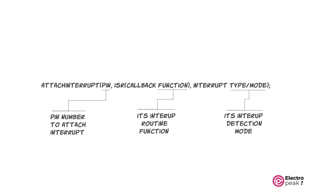
Think of an interrupt as a signal that temporarily stops normal execution, runs a short callback, and then returns to the main code. On NodeMCU, interrupts can be used on all GPIO pins except GPIO16.NodeMCU Interrupts in Arduino IDE
attachInterrupt(digitalPinToInterrupt(GPIO_Pin), IntCallback, RISING);
This syntax attaches an interrupt routine to a pin.
detachInterrupt(digitalPinToInterrupt(GPIO_Pin));
This syntax disables a pin interrupt.
Example:
Detect a rising edge on a pin and print the timestamp in milliseconds.
Interrupt Circuit Schematic of NodeMCU ESP8266 Board

NodeMCU Interrupt Code using Arduino IDE
					#include <Arduino.h>
uint8_t GPIO_Pin = D2;
volatile bool interruptTriggered = false;

void IntCallback()
{
    interruptTriggered = true;
}

void setup()
{
    Serial.begin(9600);
    attachInterrupt(digitalPinToInterrupt(GPIO_Pin), IntCallback, RISING);
}

void loop()
{
    if (interruptTriggered)
    {
        interruptTriggered = false;
        Serial.print("Stamp(ms): ");
        Serial.println(millis());
    }
}
ESP8266 Pinout: Pins Involved at Boot
These are the pins most likely to cause boot problems if external hardware drives them to the wrong level:
- GPIO16 / D0 — HIGH at boot
- GPIO0 / D3 — boot failure if pulled LOW
- GPIO2 / D4 — HIGH at boot, boot failure if pulled LOW
- GPIO15 / D8 — must be LOW at boot; boot failure if pulled HIGH
- GPIO3 / RX — HIGH at boot
- GPIO1 / TX — HIGH at boot, boot failure if pulled LOW
- GPIO10 / SD3 — HIGH at boot
- GPIO9 / SD2 — HIGH at boot
If a project suddenly stops booting after you add a module, sensor, or relay, check these pins first.
ESP8266 Pinout: Control Pins
These pins control chip enable, reset, boot mode, and wake behavior.
EN Pin (Enable)
The ESP chip is active when EN is HIGH. When EN is LOW, the chip enters minimum power consumption mode. Some modules label this pin CH_PD.
RST pin (Reset)
RST is HIGH by default. Pulling it LOW resets the ESP8266 immediately, equivalent to pressing the reset button.
FLASH/ D3/GPIO0 Pin
If you hold this pin LOW and reset or power-cycle the ESP8266, the chip enters the UART bootloader used for flashing.
This pin has the same role as the FLASH button on the board.
WAKE / GPIO16 / D0 Pin
GPIO16 can wake the ESP8266 from deep sleep. To use that feature, connect GPIO16 to RST.
When the deep-sleep timer expires, GPIO16 pulses LOW and triggers reset through RST, which wakes the board. This pin is also HIGH at boot.
ESP8266 Pinout: Power Line Pins
Power wiring is another place where confusion between board variants causes trouble, so check the actual board you have before applying external voltage
The power pins are shown below.
Warning
VIN accepts an external DC supply. Most NodeMCU boards use an AMS1117-3.3 regulator with a 5V to 10V input range. 5V is the safest and most common choice; higher voltages increase regulator heat. Verify your specific board schematic.

- Vin: Main external DC input besides USB. Most NodeMCU boards accept 5V to 10V through the onboard regulator. 5V is the safest and most common choice.
- GND: Ground.
- 3v3: Output of the onboard regulator. Budget no more than a few hundred milliamps for external peripherals; the ESP8266 itself can draw 300–400 mA during WiFi transmission. For loads above ~100 mA, use an external 3.3 V supply with common ground.
- 5V*: On LoLin (V3) boards, pin 3 is a 5 V output from the USB input. On Amica/DoIT (V2) boards, pin 3 is labeled RSV (reserved) and is not connected.
Programming NodeMCU ESP8266 in Arduino IDE
Pin selection is the main focus of this article, but once the hardware is wired, Arduino IDE setup is simple. If you want a broader module-focused walkthrough, this ESP8266 WiFi module on Arduino IDE guide is also useful.
Hardware Components
| NODEMCU ESP8266 | × | 1 |
|---|

If you need a USB-C variant in the same board family, the NodeMcu Lua ESP8266 WiFi development board with CP2102 and Type-C follows the same basic NodeMCU use case.
Software
| Arduino IDE |
|---|
Configuring Arduino IDE Software for NodeMCU
- Download and install Arduino IDE.
- Open File > Preferences.

- Paste this URL into the additional boards manager field, then click OK:
http://arduino.esp8266.com/stable/package_esp8266com_index.json - Go to Tools > Board > Board Manager. Search for ESP8266, find ESP8266 by ESP8266 community, and install it.

- Select your target board from Tools > Board > ESP8266 Boards. Choose NodeMCU 1.0 (ESP-12E Module) for most Amica/DoIT and LoLin V3 boards.
After that, you can program both ESP8266 modules and NodeMCU ESP8266 development boards in Arduino IDE.
Conclusion
The practical way to use the ESP8266 pinout is to separate chip behavior from board behavior. On NodeMCU boards, D1 and D2 are usually the safest GPIO choices, D5–D7 are good when SPI is free, and D3, D4, D8, RX, and TX need extra care because of boot or serial behavior.
For analog work, remember the difference between the raw ESP8266 ADC input and the NodeMCU A0 input. For digital work, check boot-sensitive pins before connecting relays, buttons, or sensors. If you do that, the NodeMCU ESP8266 pinout becomes predictable and easy to use.
FAQ
Which ESP8266 NodeMCU pins are safest to use for general digital I/O?
D1 (GPIO5) and D2 (GPIO4) are the safest general-purpose choices on a NodeMCU ESP8266 board. They are the best starting point for LEDs, buttons, and sensors because they have no boot restrictions or flash/serial conflicts.
Which ESP8266 pins can stop the board from booting if pulled to the wrong level?
The main boot-sensitive pins are D3/GPIO0, D4/GPIO2, D8/GPIO15, and TX/GPIO1. GPIO0 and GPIO2 fail if pulled LOW during boot, while GPIO15 fails if pulled HIGH and GPIO1 can also stop boot if pulled LOW.
Is the ESP8266 ADC range 0–1V or 0–3.3V on NodeMCU boards?
Both values apply to different contexts. The bare ESP8266 chip or module ADC is 0–1V, while the NodeMCU development board A0 input is 0–3.3V because the board adds resistive scaling.
Can I use GPIO0, GPIO2, or GPIO15 with relays, buttons, or sensors?
Yes, but only with care. GPIO0, GPIO2, and GPIO15 affect boot mode, so attached hardware must not force the wrong logic level during reset or power-up. Relays, transistor drivers, and some sensors often cause trouble here if they pull the line too early.
Which pins are used for I2C, and can I move I2C to different GPIOs on ESP8266?
The common default pair on NodeMCU is D2 (GPIO4) for SDA and D1 (GPIO5) for SCL. ESP8266 I2C can also be remapped in software, so you can move SDA and SCL to other GPIOs using Wire.begin(SDA, SCL).
Which pins are reserved for flash memory and should not be used?
GPIO6 through GPIO11 are generally reserved for the onboard flash interface and should be avoided on NodeMCU boards. These pins handle internal flash communication, so using them for external wiring can interfere with normal operation or make the board unusable.
What is the difference between ESP8266, ESP-12F, and NodeMCU?
ESP8266 is the microcontroller family. ESP-12F is a module built around that chip, adding flash and RF hardware. NodeMCU is a development-board implementation around ESP8266 modules, usually with USB serial, power regulation, headers, and easier access to GPIO pins.
Why does my NodeMCU fail to upload or boot after I connect external hardware?
The most common cause is using a boot-sensitive or serial pin for the attached hardware. If your board stops booting or uploading, first inspect GPIO0, GPIO2, GPIO15, RX, and TX, then check whether the connected device is pulling one of those pins to the wrong level during startup.